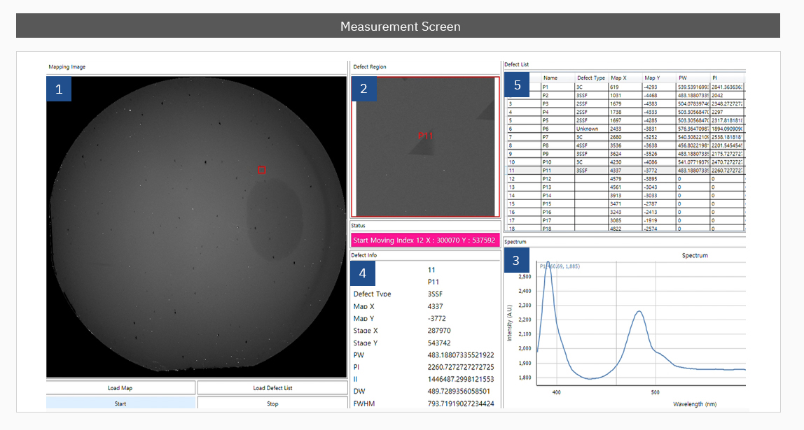
Skip to content

ELECTRIC POWER DEVICE

ELECTRIC POWER DEVICE

MiPLATO-SiC

SiC Micro Photoluminescence mapping system

Features.​

• Simultaneous measurement of 3-channel photoluminescence and 1-channel DIC laser microscopy using a 355nm laser source
• Deep learning for defect analysis
• DIC Laser Microscopy Surface Inspection
  – Reflected DIC laser microscope of excitation source (355nm)
  – Carrot, Scratch, Droplets, 3-C triangular defects
• Band edge PL inspection method, additional 2 types of data for user reference
  – BPD, Shockley stacking faults, Bar type stacking faults
• Photoluminescence spectral mapping with spectrometer
  – Whole wafer mapping
  – Spectroscopic analysis for aimed area in map data
• Auto-Navigation Function
  – Auto-defect inspection using spectral measurement using PMT mapping and image processing result
  – Exact stacking faults classification by spectrum analysis

Optical Configuration .

• Spiral scan with 1800 RPM (Max) rotation stage
  – One head type & Two head type (under development)
• Micro PL with 50x objective lens
  – 2um beam size
• Multi detectors :
  – Default : reflected DIC, Band – edge PL, Spectrometer
Two additional customer designed PL defectors

Spectrum mapping (Macro) .​

• Macro mapping for substrate & Epi-wafer can be used for QC
  – Growth machine to machine
  – Ingot to ingot
  – Wafer to wafer in ingot
  – Wafer uniformity
     > 5 mins/ 6” with 3mm step

Spectrum mapping (Micro).​

Auto-Navigation function.

• screen capture image of spectrum acquisition process
   1. Mapping Image by PMT
   2. Cropped Imgae of SF being measured
   3. Spectrum ddata of SF
   4. Detailed information of SF from spectrum
   5. Report of Classified SFs

Mapping Result.

General Specification.​

Scan method Spiral scan with 1800 RPM rotation and linear motion
Laser 20mW 355nm CW Laser
* Beam size on surface : 2um diameter thru 50x objective lens
Detector 4 PMTs, 1 Spectrometer
Stage XY-axis Linear stage
R stage with 1800RPM (Max)
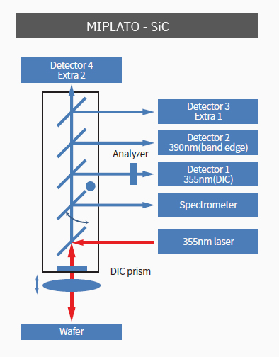
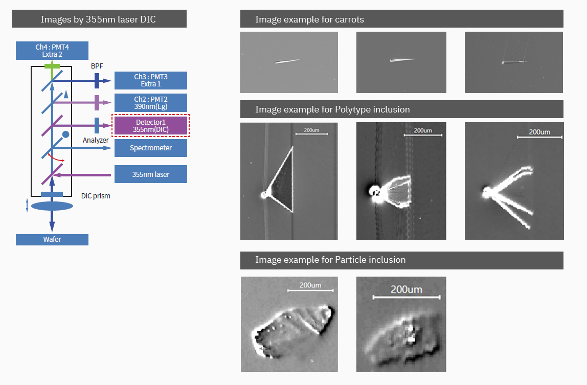
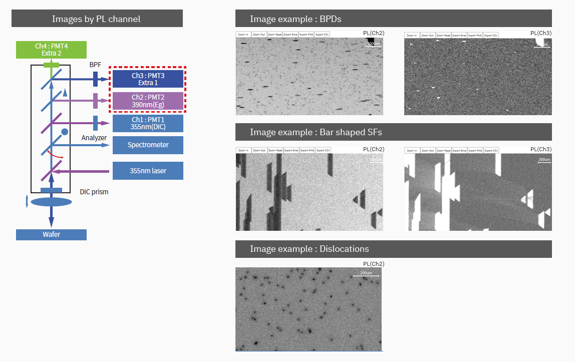
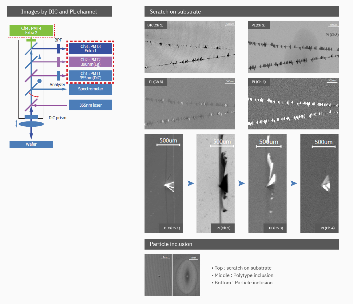
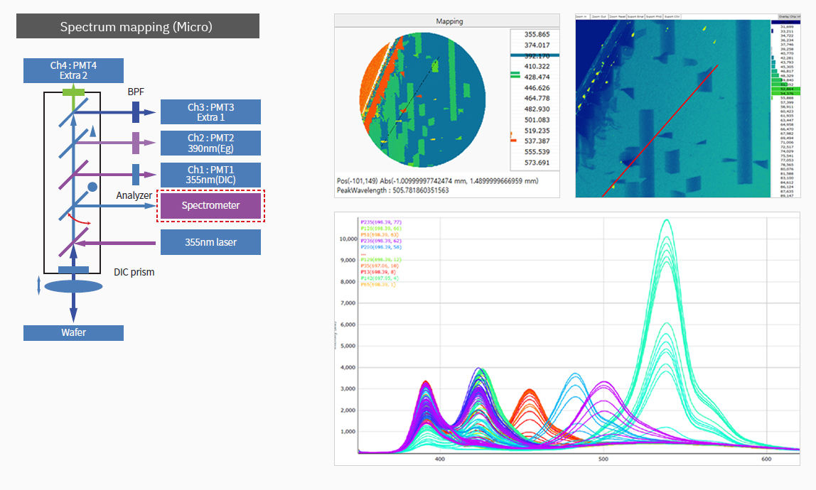
Measurement PMT1 DIC 355 Laser line for surface inspection
PMT 2,3,4 PL Port 2 (PMT 2) : PL Inspection with 390nm bandpass filter
PL Port 3 (PMT 3) : 420 nm ~ 500 nm default.
But customer choose bandpass filter between these range
PL Port 4 (PMT 4) : 3C triangular defects with 540 nm bandpass
CCD camera Image of designated position in analysis process
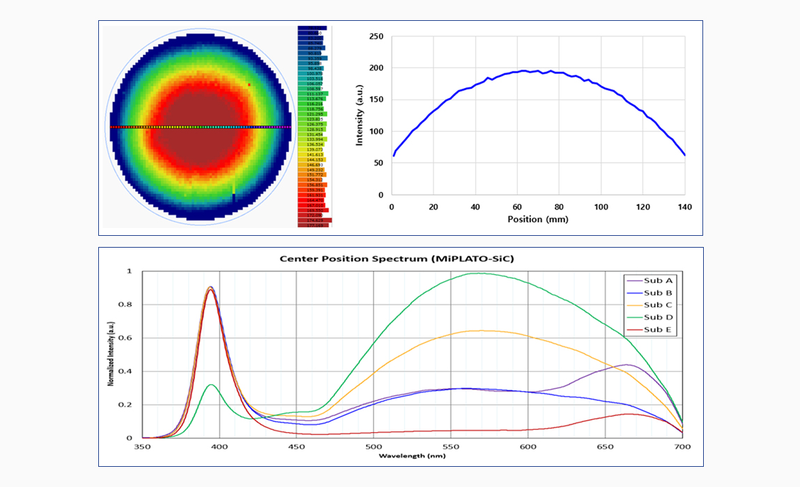
Spectrometer Spectrum between 380 nm ~ 700 nm
Detailed defects analysis, Macroscopic wafer deep level mapping
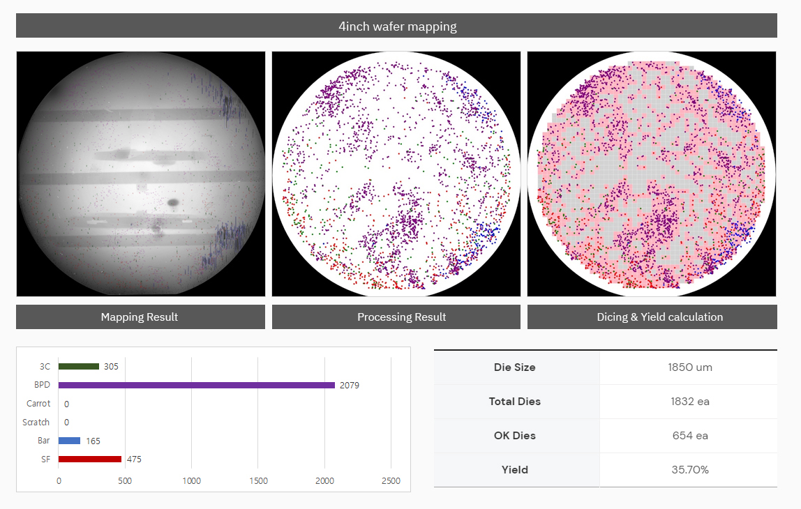
Measurement speed   4inch 6inch
PMT Mapping
(4 channel at same time,
5um step)
8pcs / 1H 6pcs / 1H
16pcs / 2H 12 pcs / 2H
Spectrometer mapping
3mm step
  5 min
Dimension (mm) 2000 (w) x 1400 (d) x 2000 (h)

Utility.

Operating
Environment
PlaceClean Room (class ~ 10000)
Temperature15 ~ 35° C
Humidity< 85 % RH with no condensation
UtilityDimensions1500 mm x 2000 mm x 2300 mm, incl. HEPA filter
Weight1760 kg
Input Voltage220V± 10% 50 / 60Hz single phase
Full load current47A
Vacuum140L / min, -80KPa
Pipe size : Outer diameter 6mm
Vacuum2120L / min, -40KPa
Pipe size : Outer diameter 6mm
Air90L / min, 0.5MPa
Pipe size : Outer diameter 6mm